yKiCad is a free, open-source software suite for electronic design automation (EDA). It is commonly used to design printed circuit boards (PCBs). It provides schematic imaging, PCB layout, and other tools for electronics experts, enthusiasts, and professional developers.
Key characteristics of KiCad:
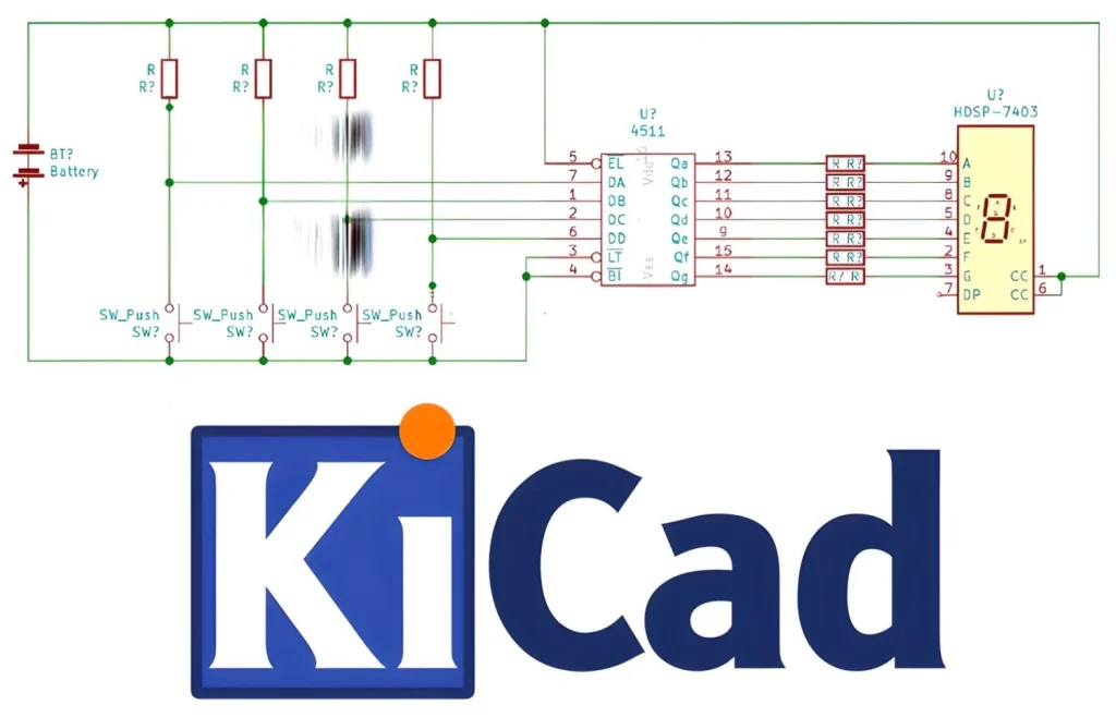
KiCad allows users to construct schematics, which are electrical circuit diagrams that show component connections. The schematic editor supports hierarchical layouts and multi-page schematics, making it ideal for complex circuits. KiCad includes libraries of symbols for many electronic components, and users can develop their own symbols for unique elements.
After creating a schematic, users can export it to the PCB layout editor. This program allows you to place components on a board, construct traces (conductive routes between components), and create layers. KiCad includes a 3D viewer that displays a visual representation of the finished board, including all components and layers. It can support up to 32 copper layers, which is excellent for highly complicated designs.
KiCad provides broad libraries for schematic symbols and PCB footprints. Users can also download third-party libraries or design their own bespoke components. The software can import and export designs in a variety of file formats, making it compatible with numerous manufacturing tools and workflows.
The Electrical Rules Review (ERC) and Design Rules Review (DRC)
ERC tests for schematic problems, such as missing connections or faulty wiring, whereas DRC checks for physical design issues, such as incorrect trace widths or spacing violations. These checks guarantee that the design is buildable and works as planned.
KiCad’s 3D viewer lets users visually review their PCB designs before production. It provides a realistic representation of the assembled board, making it easier to check the layout and component placement.
KiCad supports simulation by integrating with SPICE tools to model circuit behaviour. This enables users to evaluate the performance of their designs before manufacturing.
KiCad supports multiple operating systems, including Windows, macOS, and Linux. Its open-source nature has attracted a large and active community of developers and users who help to improve and expand the software’s features.
Advantages of KiCad:
No cost: KiCad is open source and entirely free, unlike many commercial EDA programs. It is open to everyone, from students to professional engineers.
KiCad is scalable for both tiny hobby projects and complex, multi-layer PCB designs in commercial goods.
Users can customise the software by creating custom symbols, footprints, and rules to meet their specific design demands.
KiCad’s growing user base provides substantial online documentation, tutorials, and community help through forums and GitHub, facilitating learning and troubleshooting.
KiCad’s free edition allows for unlimited design size, making it ideal for large or complex projects.
Disadvantages and challenges
KiCad can be challenging for newcomers unfamiliar with PCB design or EDA tools, despite its user-friendly interface. Some software features, such as building bespoke components, can be time-consuming.
KiCad does not have a built-in autorouter to route PCB traces automatically. However, other tools can be integrated.
KiCad may lack specific sophisticated capabilities found in commercial EDA tools, such as integrated thermal analysis and real-time collaboration.
Conclusion:
KiCad is a sophisticated open-source tool that provides a complete PCB design solution. Its versatility, scalability, and affordability make it a popular choice for enthusiasts, educators, and professionals. Although there may be a learning curve, particularly for novice users, the software’s ongoing development and helpful community help overcome these challenges, making it an excellent choice for electronics projects large and small.